Series Regulated Power Supply
Published by Arun Isaac on
Tags: electronics

Figure 1: Power Supply - PCB
This series regulated power supply provides an output voltage of about 5.3 V and a maximum current of almost 500 mA. The primary purpose of this design was as a means of independence from the college’s labs. Though we had acquired permission to use the college’s labs for our own purposes, we thought it was a good idea to slowly try and become independent of the college. In any case, independence would be necessary once the BE course was over and we were left to fend for ourselves. Also, from a HAM point of view, the idea of developing a power supply was interesting.
The design is just the standard design available in “Electronic Devices and Circuit Theory - Robert Boylestad & Louis Nashelsky” and “Electronic Devices - Floyd”. The design is essentially the result of hacking the example circuits in the two books.
The transformer steps down the power supply from 230 V AC supply to around 7 V AC and has a maximum current rating of 500 mA.
Transistor CL100 is the regulating transistor series dividing the voltage between the load and itself. Its maximum collector current is 1 A. Transistor 2N3055 with a maximum collector current rating of 15 A was considered but the idea was later dropped due to its large size, difficulty in soldering to the pcb, heat sink requirements, and general needlessness in this case where our maximum load current is just 0.5 A.
Transistor BC107 serves as the error amplifier transistor. It has a maximum collector current rating of 200 mA and was thought to be easily capable of controlling the base current of CL100. Hence it was chosen. The resistor divider of the sampling network determines the factor by which the zener voltage is multiplied to get the load voltage. The resistor divider does not work out in an all too ideal fashion, but perhaps things could have been better if a third resistor was used in parallel to Vbe of BC107. This would have served to limit the non-linear nature of the zener diode and the transistor and also possibly to reduce the load on the zener. Thus had this resistor been used, there probably would have been an improved regulation and also an increased output voltage. Also it could have helped to reduce the load on the zener, if the overall resistance of the sampling path had been higher.
Transistor SL100 forms the foldback circuit. The design was intended to fold back the current at around 0.5 A. However, there is probably something wrong with the design or our understanding of foldback circuits. For whatever reason, the power supply doesn’t seem to be folding back when the load current has exceeded the designed maximum current. However, current limiting is working out fine, and hence the foldback circuit not working is not so much of an immediate concern.
As can be seen from the VI curve of the power supply, the quality of regulation isn’t awesome, especially when it comes to high current drawing applications and even more so in burst current drawing applications such as power amplifiers. Still, considering that this is our first fully finished power supply unit (to the extent of pcb and housing!), this is understable. Improvements to this fundamental design will have to be made later when the universe permits.
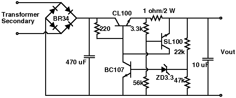
Figure 2: Power Supply
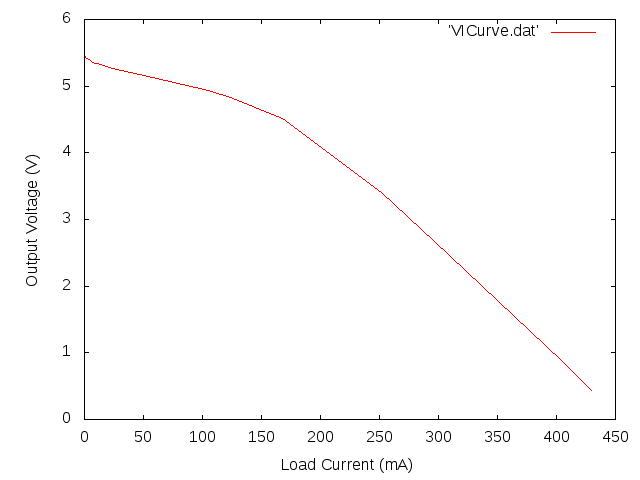
Figure 3: VI Curve of the power supply
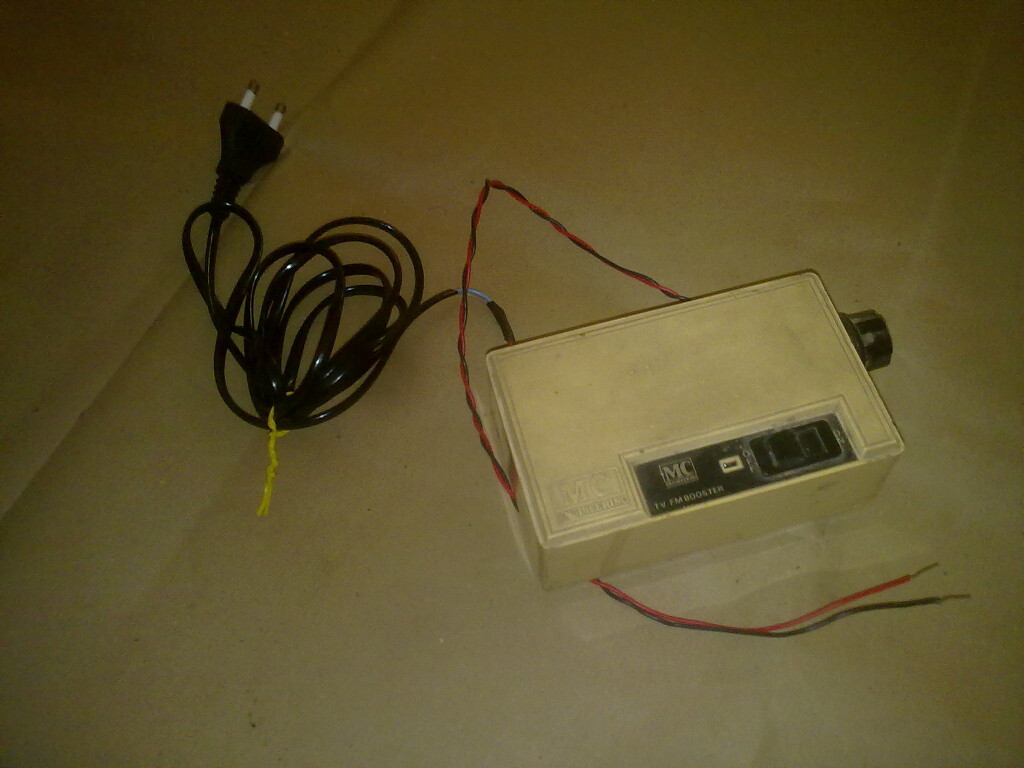
Figure 4: Completed power supply
 All content is licensed under a